
| Home | Introduction | Conventions | Implementation |
| License | Download | Contributors | Masthead |
| uCore Introduction |
| Summary |
| Philosophy |
| Block Diagram |
| Hardware Architecture |
| Instruction Architecture |
| Instruction Semantics |
| Core Registers |
| Memory Mapped Registers |
| Booting |
| Interrupts |
| Exceptions |
| Data Memory Access |
| The Instruction Cycle |
| MicroCore Scaling |
| Software Development |
| Project Status |
| Licensing |
| Acknowledgements |
| Bibliography |
| Exits |
| Fachhochschule Aargau |
| Forth-Gesellschaft eV |
| Commercial Exits |
| Send GmbH |
| Email Us |
| office@microcore.org |
| © 1999-2005 |
| Maintained by JRABnet |
MicroCore
a
scalable,
dual Stack,
Harvard Processor
for embedded Control
that fits into FPGAs easily
Klaus.Schleisiek AT freenet.de
Using an FPGA based simple and extensible processor core as the foundation of a system eventually frees the "core aided programmer" from the limitations of any static processor architecture, be it CISC, RISC, WISC, FRISC or otherwise. No more programming around known hardware bugs. A choice can be made as to whether a needed functionality should be implemented in hardware or software; simply, the least complex, most energy efficient solution can be realised while working on a specific application. Building on an FPGA, time critical and perhaps complex functions can be realised in hardware in exactly the way needed by the application offloading the processor from sub-optimal inner loops.
The FPGA approach also makes the user independent from product discontinuity problems that haunt the hi-rel industry since the dawn of the silicon age. Finally: putting the core into FPGAs puts an end to one of the high-level programming language paradigms, namely the aspect of (hoped-for) portability. Once I can realise my own instruction set, I am no longer confronted with the need to port the application to any different architecture and henceforth, the only reason to adhere to a conventional programming style is the need to find maintenance programmers. Remains the need for a vendor independent hardware description language to be portable w.r.t. any specific FPGA vendor and family. To date, MicroCore has been realised in VHDL, using the MTI simulator and the Synplify and Leonardo synthesisers targeting Xilinx and Altera FPGAs. For more and up-to-date information, please refer to "www.microcore.org".
A novel feature of MicroCore are its two different inputs to react to external events:
Interrupt: An event did happen that was NOT expected by the software.
Exception: An event did NOT happen that was expected by the software.
MicroCore is not confined to executing Forth programs but it is rooted in the Forth virtual machine. MicroCore has been designed to support Forth as its "Assembler". Support for local variables (relative return-stack addressing) is cheap and seems to be all that is needed to soup up MicroCore for C. Instructions for interpreting token threaded code have been included to support Java.
Design Philosophy
MicroCore's top priority is simplicity and understandability. MicroCore is rooted in the Forth language but it is not confined to execute Forth programs - it is a pretty good general purpose processor and indexed addressing into the return stack allows easy compilation of C programs that execute efficiently.
Yet its design approach has been different from most other processor cores: Its assembler was first and it realises about 25 Forth primitives. Whereas most other processors attempt to give you the utmost in instruction diversity from a minimum of hardware, you will find some very specialised instructions of high semantic content in MicroCore, because 30 years of Forth experience have proven that these are useful primitives. Nevertheless, each instruction executes in one clock cycle.
MicroCore is not the only architecture that uses Forth as its assembler. I took Chuck Moores NC4000 as a model, enhanced it to become the FRP1600, which never made it beyond second silicon and its vectored interrupt bug. A fresh approach was the realisation of the "Fieldbus Processor" IX1 that still sells in industrial automation. It introduced the Harvard Architecture to Forth machines. MicroCore utilises two inventions of the Transputer, namely: Concatenation of "nibbels" to form higher precision literals followed by the instruction that consumes it, which is the enabling technology for the scalable data path width without change to the object code. Secondly the EXCEPTION signal as a hardware mechanism to deal with resource scheduling, which is the enabling technology for efficient and easy to use multi-tasking.
MicroCore attempts to be an optimum in terms of hardware complexity versus instruction semantics. There are other architectures that are simpler at the expense of instruction semantics. But then you have to execute more of those simpler instructions to get a certain job done, which leads to higher power consumption because, after all, fetching instructions from program memory tends to be the major source of power consumption in microprocessor systems.
Due to Forth's extensibility - i.e. the openness of its unconventional compiler for user modifications and extensions - the Forth standardisation process is a slow consensus building process in a large community compared to the compiler writer specialists' circles of most other languages. Forth words could be thought of as the micro cells of a software system that has been realised in order to solve a specific problem. In much the same way as application specific instructions can be added to MicroCore in VHDL to realise a more specific and complex piece of hardware. Simplicity is an indication of proper factoring and understandability is the condition for wide acceptance. Proper factoring is a matter of experience and a crave for aesthetic solutions. E.g. the "proper" building blocks for a UART may be uart_clk, uart_tx, and uart_rx. Only time and experience can tell.
In releasing MicroCore to the public, I hope that it will become a catalyst to spawn additional peripheral functions, or MicroCells, placed under the same license conditions. As the Original Developer of MicroCore I reserve the right to certify conformance of Derived Work with the Original Code. This is my only business interest in MicroCore besides using it myself in embedded systems development. In that respect, the MicroCore licensing terms are similar to the freeBSD terms and much more liberal than the ubiquitous GPL.
As long as I can not support MicroCore as a product I will not be offering a "Public" MicroCore license. Instead, the "MicroCore Exploratory License" will allow individuals, universities, and research institutes to gain experience with it. I will grant a "MicroCore Unilateral License" to any company once the support situation has been clarified.
Block Diagram
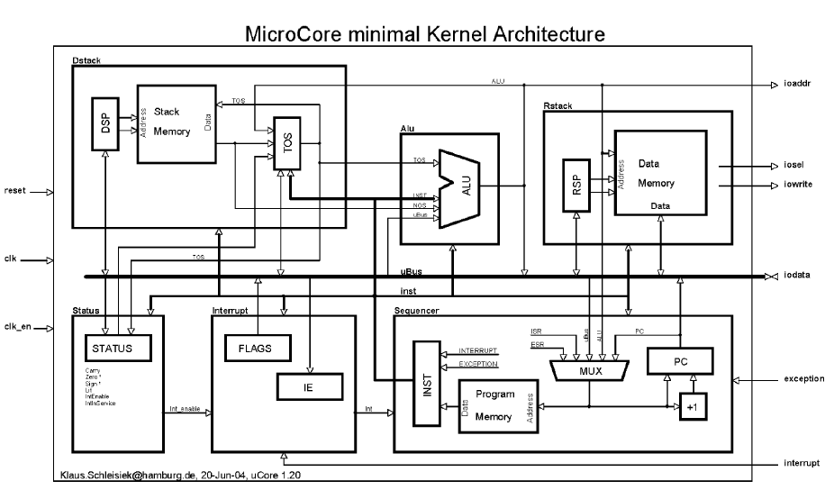
Hardware Architecture
MicroCore is a dual-stack, Harvard architecture with three memory areas that can be accessed in parallel: Data-stack (RAM), Data-memory and return-stack (RAM), and Program-memory (ROM).
The architecture diagram shows all busses that are needed. Each entity generates its own control signals from the current instruction INST and the STATUS register.
All instructions without exception are 8-bits wide, and they are stored in the program-memory ROM. Due to the way literal values can be concatenated from sequences of literal instructions, all data-paths and memories are scalable to any word width without any change in the object code as long as the magnitude of the numbers processed are representable. In essence, on a given object code the processor performs arithmetic modulo the synthesised data path width.
The data paths are made up of the data-stack Dstack, the ALU and of the data-memory and return-stack Rstack as well as of uBus, the register TOS (Top-Of-Stack), that are in between the data-stack and the ALU. Using constants in the VHDL code that work as compiler switches, the minimal MicroCore can be extended: Adding NOS (Next-Of-Stack) will allow a single cycle SWAP instruction, adding TOR (Top-Of-Return-Stack) as well will enable a single cycle, nestable decrement and branch instruction NEXT as well as complex math step instructions for multiply, divide, etc. Adding the TASK register will support a multi-tasking OS with a base-index addressing mode into a task control block. Adding indexed addressing into the return-stack will give single cycle access to local variables. Adding the IP (Instruction-Pointer) register will allow efficient interpretation of tag and token threaded code that is stored in the data memory.
The data-stack is realised by a dual-port RAM used as Stack under control of the Data-Stack-Pointer DSP, and the topmost stack item is held in the TOS register. Typically the size of the Stack Memory needed will be small enough to fit inside the FPGA. If NOS is instantiated as well, the data stack only needs single-port RAM.
IO is data-memory mapped and the most significant address bit selects the external world when set. In addition, program memory may be mapped into the lower part of the IO address space for van Neumann style read and write access. If the most significant address bit is not set data-memory and return-stack RAM is selected. The return-stack occupies the upper end of Data Memory under control of Return-Stack-Pointer RSP. Both Data and Program Memory may use internal FPGA block-RAM as "caches" and therefore, small controller applications may run in an FPGA without any external memory needs.
A number of Data Memory access instructions are available:
- Pre-incrementing absolute addressing off of an address in the TOS register with a three bit signed pre-increment in the instruction,
- Indexed addressing relative to the Return Stack Pointer for stack frame access,
- Indexed addressing relative to the TASK register.
After each memory access, the absolute memory address that had been accessed will remain in TOS. Data transfer takes place between the second data stack element and memory/IO.
The Sequencer generates the Program Memory address for the next instruction, which can have a number of sources:
- The Program Counter PC for a sequential instruction,
- the ALU for a relative branch or call,
- the TOS register for an absolute branch or call,
- the Return Stack (Data Memory) for a return instruction,
- the INSTruction register for an immediate call (soft instruction),
- the fixed Interrupt Service Routine address ISR as part of an interrupt acknowledge cycle, or
- the fixed Exception Service Routine address ESR for the EXCEPTION signal or the PAUSE instruction,
- the fixed Overflow Service Routine address OSR for a conditional overflow service routine.
The STATUS register has been shown as a separate entity. In the code however, it is composed of status bits generated from several sources and therefore, it is spread across the entire design as record stBus.
The Interrupt Processing unit takes care of synchronising and masking a scalable number of static external interrupt sources.
Both, instruction decoding and status register bit processing has been decentralised because it makes the code easier to understand, maintain, modify, and extend.
Instruction Architecture
An instruction is always 8 bits wide. Scalability is achieved on the object code level because all literal values are composed of literal instructions that can be concatenated. Refer to [3 instruction structures] for a discussion of the literal representation used, which is characterised by its "prefix" nature dubbed called "Vertical instruction set with literal prefixes" in the paper. To my knowledge, this type of code has been invented by David May for the Transputer.
It has two advantages and one drawback compared to other instruction set structures:
Each instruction is "self contained" and therefore, this type of code can be interrupted between any two instructions, simplifying interrupt hardware and minimising interrupt latency to the max.
Long literals can be composed of a sequence of literal instructions that are concatenated in the TOS register. Therefore, this type of instruction architecture is independent of the data-word width.
Prefix code has the highest instruction fetch rate compared to the two other instruction types discussed in the paper. Therefore, it is not really the technology of choice for demanding real-time applications. A way out would be to fetch several instructions per memory access but that introduces unpleasant complexity for branch destinations.
Keeping in mind that MicroCore is about putting a very simple and small processor core into FPGAs for simple, embedded control, the latter drawback is tolerable because the instruction fetch delay, even using external ROM, will hardly dominate total processor delay because all processor logic will be contained in an FPGA and therefore, it will be substantially slower than an ASIC implementation anyway.
The instruction
|
7 $80 |
6 $40 |
5 $20 |
4 $10 |
3 $8 |
2 $4 |
1 $2 |
0 $1 |
|
Lit/Op |
Type |
Stack |
Group |
||||
- Lit/Op Bit
- Type field
- Stack field
- Group field
1: 7-bit Literal (signed)
0: 7-bit Opcode
The Lit/Op field is a semantic switch:
When set, the remaining 7 bits are interpreted as a literal nibble and transferred to the Top-of-Stack (TOS) register. When the previous instruction had been an opcode, the literal nibble is sign-extended and pushed on the stack. If its predecessor was a literal nibble as well, the 7 bits are shifted into TOS from the right. Therefore, the number of literal nibbles needed to represent a number depends on its absolute magnitude.
When not set, the remaining 7 bits are interpreted as an opcode. Opcodes are composed of three sub-fields whose semantics are almost orthogonal: Type, Stack, and Group. Not all possible bit combinations of these fields have a meaningful semantic easing instruction decoding complexity.
|
Code |
Name |
Action |
|
00 |
BRA |
Branches, Calls and Returns |
|
01 |
ALU |
Binary and Unary Operators |
|
10 |
MEM |
Data-Memory and Register access |
|
11 |
USR |
Not used by core, free for user extensionsUser instructions / immediate calls |
BRAnches are conditioned on the group field and they consume the content of TOS, using either TOS or TOS+PC as destination address. Although elegant, the fact that each branch has to pop the stack to get rid of the destination address makes the implementation of Forth's IF, WHILE, and UNTIL cumbersome. Therefore, the DROP_FLAG instruction has been implemented to get rid of the flag prior to executing the branch. Calls push the content of the PC on the return-stack while branching. Returns pop the return-stack using it as the address of the next instruction.
ALU instructions use the stack as source and destination for arithmetic operations. Unary operations only use TOS, binary operations use TOS and Next-of-Stack (NOS) storing the result in TOS. Complex math step instructions use TOS, NOS and TOR.
MEMory instructions refer to the data memory when the most significant bit of TOS, which holds the address, is not set. When set, it refers to input/output operations with the external world. The return-stack occupies the upper end of data-memory and the Program Memory may be accessed at the I/O space if van Neumann addressing has been implemented. Eight internal registers can be accessed directly using the Group field.
32 USeR instructions are free for any application specific functions, which are needed to achieve total system throughput. The first four USeR instructions coincide with MicroCore's hardware vectors RESET, ISR (InterruptServiceRoutine), ESR (ExceptionServiceRoutine), and OSR (OverflowServiceRoutine). As a default, the remaining 28 instructions perform a call to 28 trap vector addresses that have room for a sequence of instructions to be used to e.g. emulate multi-cycle instructions.
|
Code |
Name |
Action |
|
00 |
NONE |
Type dependent |
|
01 |
POP |
Stack->NOS->TOS |
|
10 |
PUSH |
TOS->NOS->Stack |
|
11 |
BOTH |
Type dependent |
POP pops and PUSH pushes the data stack. The stack semantics of the remaining states NONE and BOTH depend on type and on external signals INTERRUPT and EXCEPTION. This is where the opcode fields are non-orthogonal creating instruction decoding complexity, which is gracefully hidden by the synthesiser.
|
Code |
Binary-Ops ALU |
Unary-Ops ALU BOTH |
Complex-Math ALU NONE |
Conditions BRA |
Branches BRA PUSH |
Registers MEM |
|
000 |
ADD |
NOT |
MULTS |
NEVER |
DUP |
STATUS |
|
001 |
ADC |
SL |
0DIVS |
ALWAYS |
EXC |
TOR |
|
010 |
SUB |
ASR |
UDIVS |
ZERO |
QDUP |
RSTACK |
|
011 |
SSUB |
LSR |
not used |
NZERO |
QOVL |
LOCAL |
|
100 |
AND |
ROR |
LDIVS |
SIGN |
INT |
RSP |
|
101 |
OR |
ROL |
not used |
NSIGN |
IRET |
DSP |
|
110 |
XOR |
ZEQU |
not used |
NOVL |
THREAD |
TASK |
|
111 |
NOS |
CC |
SWAPS |
NCARRY |
TOKEN |
IP |
Instructions that are not available in the minimal implementation are set in italics.
The semantics of the group field depend on the type field and in the case of ALU and BRA also on the stack field.
Of the binary operators NOS is used to realise OVER and NIP.
Unary operations are detailed below.
Of the conditions, NEVER is used to realise NOP, DUP and DROP. NZERO supports the use of the Top-Of-Return-stack as a loop index. PAUSE and INT are conditions to aid in processing external events INTERRUPT and EXCEPTION.
Of the registers, TOR is used to implement R@, whereas RSTACK implements >R and R>.
Instruction Semantics
In the following tables the LIT-field is marked with - and +.
This indicates the following two cases:
-: The previous instruction has also been an opcode; TOS holds the top-of-stack value.
+: The previous instruction(s) have been literals; TOS holds a "fresh" literal value.
- BRA instructions
- ALU instructions
- MEM instructions
- USR instructions
- Complex Branches (BRA PUSH)
- Unary Math Instructions (ALU BOTH)
- Complex Math (ALU NONE)
- Instruction Mnemonics
|
LIT |
Stack |
act |
Operation |
Forth operators / phrases |
|
* |
none |
none |
conditional return from subroutine When Cond=ZERO or NZERO Stack -> NOS -> TOS |
EXIT NOP ?EXIT 0=EXIT |
|
- |
pop |
conditional branch to Program[TOS] Stack -> NOS -> TOS |
absolute_BRANCH |
|
|
+ |
pop |
conditional branch to Program[PC+TOS] Stack -> NOS -> TOS |
relative_BRANCH |
|
|
* |
push |
Complex branches, see below |
DUP ?DUP INTERRUPT IRET EXCEPTION ?OVL |
|
|
- |
both |
pop push |
conditional call to Program[TOS] Stack -> NOS -> TOS |
absolute_CALL DROP |
|
+ |
both |
pop push |
conditional call to Program[PC+TOS] Stack -> NOS -> TOS |
relative_CALL DROP |
|
Stack |
act |
Operation |
Forth operators / phrases |
|
none |
none |
Complex math instructions, see below |
SWAP |
|
pop |
Stack -> NOS <op> TOS -> TOS |
+ - AND OR XOR NIP |
|
|
push |
NOS <op> TOS -> TOS TOS -> NOS -> Stack |
2DUP_+ OVER |
|
|
both |
none |
TOS <uop> -> TOS Unary math instructions, see below |
0= 2* ROR ROL 2/ u2/ |
|
Stack |
act |
Operation |
Forth operators / phrases |
|
none |
pop |
Stack -> NOS -> TOS -> Register LOCAL := Stack -> NOS -> Data[RSP+TOS] TASK := Stack -> NOS -> Data[TASK+TOS] |
>R, R! store into local variables store into task variables |
|
pop |
Stack -> NOS -> Data[TOS+<inc>] TOS + <inc> -> TOS |
! pre-incrementing data memory or I/O store |
|
|
push |
Data[TOS+<inc>] -> NOS -> Stack TOS + <inc> -> TOS |
@ pre-incrementing data memory or I/O fetch |
|
|
both |
push |
Register -> TOS -> NOS -> Stack LOCAL := Data[RSP+TOS] -> NOS -> Stack TASK := Data[TASK+TOS] -> NOS -> Stack |
R@, R> fetch from local variables fetch from task variables |
By default, the USR instructions perform an immediate call to the following vector address:
vector_addr = instruction(4..0) * usr_vect_width
Therefore, each trap vector has room for usr_vect_width instructions.
Four trap vectors are used by MicroCore itself:
0: Reset
1: ISR: Interrupt Service Routine
2: ESR: Exception Service Routine
3: OSR: Overflow Service Routine
|
DUP |
TOS -> TOS -> NOS -> Stack |
|
QDUP |
Performs a DUP when TOS is non-zero, otherwise does nothing |
|
QOVL |
Performs a call to the overflow service routine when the overflow status bit is set |
|
IRET |
Performs an EXIT and restores the status register from TOS |
|
THREAD |
Threaded code interpreter. IF Data[IP] < 0 THEN (most significant bit set) Program_Address <- Data[IP] IP <- IP+1 ELSE PC <- Program_Address - 1 IP <- Data[IP] Stack <- NOS <- TOS <- IP+1 END IF The two instruction sequence "THREAD >R" is a tag threaded code interpreter. When the most significant bit is set, the remaining bits are an address of the code to be executed. When the most significant bit is not set, it is the address of another threaded code definition. The sequence "THREAD >R" will be automatically repeated until an executable code sequence is located, pushing return addresses on the return stack appropriately. |
|
TOKEN |
Token threaded code interpreter. The two instruction sequence "THREAD TOKEN" is a token threaded code interpreter. IF IP = address within token table THEN Program_Address <- Data[IP] IP <- TOS <- NOS <- Stack ELSE >R END IF |
|
SL |
Shift Left |
0 -> LSB, MSB -> C |
|
ASR |
Arithmetic Shift Right |
MSB -> MSB-1, LSB -> C |
|
LSR |
Logical Shift Right |
0 -> MSB, LSB -> C |
|
ROR |
ROtate Rigth |
C -> MSB, LSB -> C |
|
ROL |
ROtate Left |
C -> LSB, MSB -> C |
|
ZEQU |
Zero EQUals |
When TOS=0, true -> TOS, otherwise false -> TOS |
|
CC |
Complement Carry |
not Carry -> Carry |
When both NOS and TOR are implemented, complex math step instructions are available.
MULTS is a step instruction for an unsigned multiply of two numbers producing a double precision product. The multiplicand must be in NOS, the multiplier must be in TOR and the product builds up in TOS || TOR.
Macro: umultiply ( mult1 mult2 -- prod_l prod_h )
>r 0 #data_width 0 ?DO mults LOOP nip r> ;
generates code for a multi cycle U* instruction, which is independent of the data word width. U* may be interrupted at any time.
0DIVS, UDIVS, LDIVS are step instructions for an unsigned divide of a double precision dividend by a divisor, producing a single precision quotient and the remainder. When the result does not fit into the quotient, the overflow status bit will be set.
Macro: udivide ( div_l div_h divisor -- rem quot )
0divs #data_width 0 ?DO udivs LOOP ldivs nip r> ;
generates code for a multi cycle UM/MOD instruction, which is independent of the data word width. In order to execute the UDIVS instruction, the divisor must be in NOS, div_l must be in TOR and div_h must be in TOS. 0DIVS takes care of this parameter set up clearing the overflow bit as well. Each division step must take into account the most significant bit of the previous step and therefore, a final step LDIVS is needed to produce a valid quotient and to check for overflow. UM/MOD may be interrupted at any time.
\ Conditional exits
NEVER NONE BRA Op: nop ( -- )
ALWAYS NONE BRA Op: exit ( -- )
ZERO NONE BRA Op: z-exit ( flag -- )
NZERO NONE BRA Op: nz-exit ( flag -- )
SIGN NONE BRA Op: s-exit ( -- )
NSIGN NONE BRA Op: ns-exit ( -- )
NOVL NONE BRA Op: no-exit ( -- )
NCARRY NONE BRA Op: nc-exit ( -- )
\ Conditional branches
NEVER POP BRA Op: drop_flag ( flag brn_addr -- brn_addr )
ALWAYS POP BRA Op: branch ( brn_addr -- )
ZERO POP BRA Op: z-branch ( brn_addr -- )
NZERO POP BRA Op: nz-branch ( brn_addr -- )
SIGN POP BRA Op: s-branch ( brn_addr -- )
NSIGN POP BRA Op: ns-branch ( brn_addr -- )
NOVL POP BRA Op: no-branch ( brn_addr -- )
NCARRY POP BRA Op: nc-branch ( brn_addr -- )
\ Conditional calls
NEVER BOTH BRA Op: drop ( n -- )
ALWAYS BOTH BRA Op: call ( brn_addr -- )
ZERO BOTH BRA Op: z-call ( brn_addr -- )
NZERO BOTH BRA Op: nz-call ( brn_addr -- )
SIGN BOTH BRA Op: s-call ( brn_addr -- )
NSIGN BOTH BRA Op: ns-call ( brn_addr -- )
NOVL BOTH BRA Op: no-call ( brn_addr -- )
NCARRY BOTH BRA Op: nc-call ( brn_addr -- )
\ Complex branches
DUP PUSH BRA Op: dup ( n -- n n )
EXC PUSH BRA Op: exc ( -- )
QDUP PUSH BRA Op: ?dup ( n -- n n | 0 )
QOVL PUSH BRA Op: ?ovl ( -- )
INT PUSH BRA Op: int ( -- status )
IRET PUSH BRA Op: iret ( status -- )
THREAD PUSH BRA Op: thread ( -- ip_addr )
TOKEN PUSH BRA Op: token ( ip_addr -- )
\ Binary operators
ADD POP ALU Op: + ( n1 n2 -- n1+n2 )
ADC POP ALU Op: +c ( n1 n2 -- n1+n2+carry )
SUB POP ALU Op: - ( n1 n2 -- n1-n2 )
SSUB POP ALU Op: swap- ( n1 n2 -- n2-n1 )
AND POP ALU Op: and ( n1 n2 -- n1_and_n2 )
OR POP ALU Op: or ( n1 n2 -- n1_or_n2 )
XOR POP ALU Op: xor ( n1 n2 -- n1_xor_n2 )
NOS POP ALU Op: nip ( n1 n2 -- n2 )
ADD PUSH ALU Op: 2dup + ( n1 n2 -- n1 n2 n1+n2 )
ADC PUSH ALU Op: 2dup +c ( n1 n2 -- n1 n2 n1+n2+carry )
SUB PUSH ALU Op: 2dup - ( n1 n2 -- n1 n2 n1-n2 )
SSUB PUSH ALU Op: 2dup swap- ( n1 n2 -- n1 n2 n2-n1 )
AND PUSH ALU Op: 2dup and ( n1 n2 -- n1 n2 n1_and_n2 )
OR PUSH ALU Op: 2dup or ( n1 n2 -- n1 n2 n1_or_n2 )
XOR PUSH ALU Op: 2dup xor ( n1 n2 -- n1 n2 n1_xor_n2 )
NOS PUSH ALU Op: over ( n1 n2 -- n1 n2 n1 )
\ Unary Operators
NOT BOTH ALU Op: invert ( n1 -- n2 )
SL BOTH ALU Op: 2* ( n1 -- n2 )
ASR BOTH ALU Op: 2/ ( n1 -- n2 )
LSR BOTH ALU Op: u2/ ( n1 -- n2 )
ROR BOTH ALU Op: ror ( n1 -- n2 )
ROL BOTH ALU Op: rol ( n1 -- n2 )
ZEQU BOTH ALU Op: 0= ( n1 -- flag )
CC BOTH ALU Op: cc ( -- )
\ Complex Math Steps
MULTS NONE ALU Op: mults ( u1 u2 -- u1 u3 )
0DIVS NONE ALU Op: 0divs ( ud1 u2 -- u2 u3 )
UDIVS NONE ALU Op: udivs ( u2 u3 -- u2 u3' )
LDIVS NONE ALU Op: ldivs ( u2 u3 -- u2 u3' )
SWAPS NONE ALU Op: swap ( n1 n2 -- n2 n1 )
\ Data Memory access
N PUSH MEM Op: +ld ( addr -- n addr+n )
N POP MEM Op: +st ( n addr -- addr+n )
\ Internal Register access
STATUS BOTH MEM Op: status@ ( -- status )
TOR BOTH MEM Op: r@ ( -- n )
RSTACK BOTH MEM Op: r> ( -- n )
LOCAL BOTH MEM Op: +lld ( index -- n rstack+index )
RSP BOTH MEM Op: rsp@ ( -- rstack_addr )
DSP BOTH MEM Op: dsp@ ( -- dstack_addr )
TASK BOTH MEM Op: +tld ( index -- n task+index )
IP BOTH MEM Op: ip@ ( -- addr )
STATUS NONE MEM Op: status! ( status -- )
TOR NONE MEM Op: r! ( n -- )
RSTACK NONE MEM Op: >r ( n -- )
LOCAL NONE MEM Op: +lst ( n index -- rstack+index )
RSP NONE MEM Op: rsp! ( rstack_addr -- )
DSP NONE MEM Op: dsp! ( dstack_addr -- ? )
TASK NONE MEM Op: +tst ( n index -- task+index )
IP NONE MEM Op: ip! ( addr -- )
Core Registers
- STATUS
- TOR
- RSTACK
- LOCAL
- RSP
- DSP
- TASK
- IP
|
Bit |
Name |
Access |
Description |
|
0 |
C |
R/W |
The Carry-Flag reflects the result of the most recent ADD, ADC, SUB, SSUB, SL, ASR, LSR, ROR, and ROL instructions. When subtracting, it is the complement of the borrow bit. |
|
1 |
OVL |
R/W |
The Overflow-Flag reflects the result of the most recent ADD, ADC, SUB, SSUB, UDIVS, and LDIVS instructions. |
|
2 |
IE |
R/W |
Interrupt-Enable-Flag |
|
3 |
IIS |
R/W |
The Interrupt-In-Service-Flag is set at the beginning of an interrupt-acknowledge cycle. It is reset by the IRET (Interrupt-RETurn) instruction. When IIS is set, interrupts are disabled. When the Status-register is read, IIS always reads as '0'. |
|
4 |
LIT |
R |
The LITeral-Status-Flag reflects the most significant bit of the previous instruction. |
|
5 |
N |
R |
The Negative-Flag reflects the content of the most-significant-bit of TOS or of NOS when LIT=1 |
|
6 |
Z |
R |
The Zero-Flag reflects the content of TOS or of NOS when LIT=1 |
Z and N reflect the actual state of the top "number" on the stack. This may be in TOS (when LIT=0) or in NOS (when LIT=1) because e.g. a target address may be in TOS.
For the ordering of the bits it has been taken into consideration that "masks" for masking off flags can be loaded with only one literal nibble. This is important for the C- and IE-flags, see below.
Top-Of-Return-stack. This allows access to the return-stack without pushing or popping it.
Return-STACK. When RSTACK is used as a destination, a return-stack push is performed. When it is used as a source, a return-stack pop is performed.
This register-addressing mode (MEM NONE LOCAL and MEM BOTH LOCAL) is included in order to support C and its local variable mentality. These can be placed in a return-stack frame. The actual data memory address is the sum of RSP+TOS. After the memory access, the absolute memory address will remain in TOS.
Return-Stack-Pointer. It is used to implement the return-stack that is located at the upper end of the data memory and it can be read and written to support multi-tasking and stack-frame linkage. The return stack pointer width is defined on the VHDL level. For multi-tasking support, multiple return stacks can be instantiated extending the address to the left of the return-stack-pointer itself.
Data-Stack-Pointer. It is used to implement the data-stack and it can be read and written to support multi-tasking. The data stack pointer width is defined on the VHDL level. For multi-tasking support, multiple data stacks can be instantiated extending the address to the left of the data-stack-pointer itself.
The TASK register itself can be read and written via memory mapped I/O (address = -2). In a multi-tasking environment it would hold an address pointing at the Task Description Block (TDB) of the active task. The implementation of the multitasking mechanism is operating system dependent. Variables that are local to a task can be accessed via the MEM NONE TASK (store) and MEM BOTH TASK (fetch) instructions. The data memory address is the sum of TASK+TOS and after the memory access the absolute memory address remains in TOS.
If the TASK register is not used for multitasking support, it constitutes a general base register for a pre-incrementing base-offset addressing mode.
The IP register is used to support tag and token threaded code. See: THREAD and TOKEN in the complex branches group.
Memory Mapped Registers
- FLAGS (read) / IE (write) (-1)
- TASK register (-2)
This is a pair of registers FLAGS for reading, IE (Interrupt Enable) for writing.
An interrupt condition exists as long as any bit in FLAGS is set whose corresponding bit in IE has been set previously. Interrupt processing will be performed when the processor is not already executing an interrupt (IIS-status-bit not set) and interrupts are enabled (IE-status-bit set).
Typically at the beginning of interrupt processing (after calling the hard-wired interrupt handler address ISR) the FLAGS-register will be read. One specific bit is associated with each potential interrupt source. When a certain interrupt has been asserted, its associated bit will be set. All interrupts are static and therefore, it is the responsibility of the interrupt service routine (ISR) of a specific interrupt to reset the interrupt signal of the external hardware before the end of the ISR.
IE (Interrupt Enable) is a register, which can only be written, and it holds one enable bit for each interrupt source. Setting or resetting interrupt enable bits is done in a peculiar way, which could be called "bit-wise writing":
When IE is written, the least significant bit determines whether individual IE-bits will be set ('1') or reset ('0'). All other bits written to IE select those enable bits, which will be affected by the write operation. Those bits that are set ('1') will be written to, those bits that are not set ('0') will not be changed at all. This way individual interrupt enable bits may be changed in a single cycle without affecting other IE-bits and without the need to use a "shadow variable".
The TASK register itself can be read and written at address -2. The TASK register sets the base address for the MEM NONE TASK and the MEM BOTH TASK data memory access instructions.
Booting
Given MicroCore's hardware architecture, this is very simple:
A RESET signal resets all registers to zero. Because the code for a NOP { BRA NONE NEVER } happens to be all zeros, the processor just fetches the instruction pointed to by the PC register (which had also been reset to zero) in the first cycle. Therefore, the reset vector happens to be at memory address zero.
Interrupts
- The Interrupt Mechanism
- Handling Multiple Interrupt Sources
At first, interrupt requests are synchronised.
In the succeeding cycle(s) the following mechanism will unfold by hardware design:
1st cycle:
The current program memory address will be loaded into the PC un-incremented.
The instruction BRA PUSH INT will be loaded into the INST register instead of the output of the program memory.
2nd cycle:
Now, BRA PUSH INT will be executed that performs a CALL to the ISR-address, which is a constant address, selected by the program address multiplexer and STATUS is pushed on the data stack at the same time.
Therefore, only the first INT-cycle must be performed by special hardware. The second cycle (INT-instruction) is executed by an instruction that is forced into the INST register during the first Interrupt acknowledge cycle.
Whenever an interrupt source whose corresponding interrupt enable bit is set in the IE-register is asserted its associated bit in the FLAGS-register will be set and an interrupt condition exists. An interrupt acknowledge cycle will be executed when the processor is not currently executing an interrupt (IIS-bit not set) and interrupts are globally enabled (IE-bit of the STATUS-register set).
Please note that neither the call to the ISR-address nor reading the FLAGS-register will clear the FLAGS register. It is the responsibility of each single interrupt server to reset its interrupt signal in the external hardware as part of its interrupt service routine.
Exceptions
The Exception signal complements interrupts:
An interrupt is an event that has not been anticipated by the software currently being executed.
An exception is an event that has not (yet) happened although anticipated by the software. Therefore, the processor has to wait or - in the case of a multi-tasking environment - it would process another task.
To my knowledge, the Transputer has been the first processor to realise an exception mechanism in hardware, which was used to perform a task switch that was entirely realised in hardware. Nice as this feature and the underlying philosophy of its programming language Occam may be, it crippled the transputer for traditional programming languages. This in turn did make the transputer difficult to understand and market. It never became really popular although its users were happy with it.
Nevertheless, hardware support for multitasking seems to be an attractive feature greatly simplifying software engineering for complex systems. Analysing the real needs w.r.t. multitasking support it occurred to me that a full-blown task switch mechanism in hardware is not really needed. Instead, a mechanism that would allow to access resources that may not be ready yet using fetch and store without the need to explicitly query associated status flags beforehand is all that is needed to hide multitasking pains from the application programmer.
Therefore, MicroCore has an Exception mechanism to support multitasking or, to be less ambitious, to deal with busy resources. Fortunately, it turned out that the implementation of this mechanism in MicroCore comes almost for free and therefore, it is build into the core from the very beginning.
An additional external control input has been added: EXCEPTION. When the processor intends to access a resource, the resource may not be ready yet. In such an event, it can assert the EXCEPTION signal before the end of the current execution cycle (before the rising CLK edge). This disables latching of the next processor state in all registers but the INST register that loads BRA PUSH EXC instead of the next instruction from program memory.
In the next processor cycle, BRA PUSH EXC will be executed calling the ESR-address (Exception Service Routine).
The ESR-address will typically hold a branch to code, which will perform a task switch depending on the operating system. This may be used to emulate the Transputer. Please note that the return address pushed on the return-stack is the address of the instruction following the one that caused the Exception. Therefore, before re-activating the excepted task again, the return address on the return-stack must be decremented by one prior to executing the EXIT instruction (BRA NONE ALWAYS) in order to re-execute the instruction, which caused the exception previously. Please note that no other parameter reconstruction operation prior to re-execution is needed because the EXCEPTION cycle fully preserves all registers but the INST register.
The EXCEPTION mechanism is independent from the interrupt mechanism. It adds one cycle of delay to an interrupt acknowledge when both an interrupt request and an EXCEPTION signal coincide.
In essence, the EXCEPTION mechanism allows to access external resources without having to query status bits to ascertain the availability/readiness of a resource. This greatly simplifies the software needed for e.g. serial channels for communicating with external devices or processes.
Data Memory Access
On a data memory access, TOS holds the base address and NOS holds/receives the value to be exchanged with memory. Pre-incrementing access operators +LD and +ST have been defined. The group field is used as a signed increment spanning the range from -4 .. 3 and after the memory access, the incremented address remains in TOS.
Relative addressing into the return-stack may be used using the LOCAL "register". The actual memory address is the output of the ALU-adder, adding the offset in TOS and the RSP. After the memory access, TOS holds the physical address (pointer) of the memory access. As a further alternative, relative addressing into the data memory can be performed relative to the TASK register that points to the beginning of a block of memory that may e.g. hold variables that are local to a task.
Addresses are shown for a 16 bit data path width by way of example.
The Instruction Cycle
Due to the use of a tri-state uBus and synchronous blockRAM for the stacks and data and program memory "caches", one basic uCore instruction cycle consists of four phases and therefore, at least two input clock (sysCLK) cycles are needed for one instruction cycle.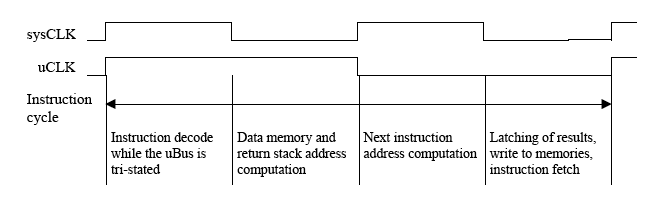
MicroCore Scaling
The values assigned to these VHDL constants are the ones used for the uCore100 prototyping board.
Important notice: Most of these settings have to be "ported" to the cross-compiler by setting Constants in the load_<application>.f file appropriately.
- Semantic Switches
- Vector Widths
CONSTANT syn_stackram : STD_LOGIC := '1';
When set to '1', the stack_ram will be relised as synchronous blockRAM. Otherwise, it will be realised as asynchronous RAM, which may be internal or external of the the FPGA.
CONSTANT with_locals : STD_LOGIC := '1';
When set to '1', the Instantiates the LOCAL addressing mode relative to the return stack pointer (RSP+TOS).
CONSTANT with_tasks : STD_LOGIC := '1';
When set to '1', the TASK addressing mode relative to the TASK register (TASK+TOS) will be instantiated. For multi-tasking, tasks_addr_width (see below) has to be set appropriately as well.
CONSTANT with_nos : STD_LOGIC := '1';
When set to '1', the NOS (Next-Of-Stack) register will be instantiated. This is needed for the single cycle SWAP instruction and the complex math step instructions.
CONSTANT with_tor : STD_LOGIC := '1';
When set to '1', the TOR (Top-Of-Return_stack) register will be instantiated. This is needed for the decrement_and_branch instruction NEXT and the complex math step instructions.
CONSTANT with_ip : STD_LOGIC := '1';
When set to '1', the IP (Instruction Pointer) register will be instantiated. This is needed for the THREAD and TOKEN instructions for interpreting threaded code.
CONSTANT with_tokens : STD_LOGIC := '1';
When set to '1', the TOKEN instruction will be instantiated, which allows rapid token threaded code interpretation.
CONSTANT data_width : NATURAL := 32;
This defines the data path width and therefore, the magnitude of the numbers that may be processed. Please note that the object code will not change as long as the magnitude of the largest number to be processed fits the data path width.
CONSTANT data_addr_width : NATURAL := 21;
This sets the address range of the data memory, which can at most be data_width-1 wide because the "upper" half of the address range is used for external memory mapped I/O.
CONSTANT dcache_addr_width : NATURAL := 0;
Number of address bits of the data memory space that is realised as block-RAM inside the FPGA.
CONSTANT prog_addr_width : NATURAL := 19;
Program memory address width sets the size of the program memory. It can be at most data_width wide because all program addresses have to fit on the return stack.
CONSTANT pcache_addr_width : NATURAL := 0;
Number of address bits of the program memory space that is realised as block-RAM inside the FPGA. When pcache_addr_width=0, no internal RAM is used; when pcache_addr_width=prog_addr_width, no external RAM is used at all.
CONSTANT prog_ram_width : NATURAL := 16;
Number of address bits that may be used to modify the program memory van Neumann style. If set to zero, the program memory operates as a pure ROM of a Harvard Architecture.
CONSTANT ds_addr_width : NATURAL := 6;
Number of address bits for the data stack memory.
CONSTANT rs_addr_width : NATURAL := 8;
Number of address bits for the return stack memory.
CONSTANT tasks_addr_width : NATURAL := 3;
Number of address bits for the task address. 2**tasks_addr_width copies of the data and the return stack will be allocated. The task address is added to the left of both the ds_address and the rs_address.
CONSTANT usr_vect_width : NATURAL := 3;
The implicit call destination addresses for two adjacent USR instructions will be 2**usr_vect_width apart from each other.
CONSTANT reg_addr_width : NATURAL := 3;
Number of address bits reserved for internal memory mapped registers that reside at the upper end of the address space.
CONSTANT interrupts : NATURAL := 2;
Number of interrupt inputs and their associated FLAGS and Interrupt-Enable bits.
CONSTANT token_width : NATURAL := 8;
Number of bits for a token address of a token threaded system.
Software Development
An interactive software development environment for MicroCore is rather straightforward and it has been realised under Linux.
A "debuggable MicroCore" has an additional umbilical interface that can be controlled by a centronics port on the PC. The program memory, which must be realised as a RAM, can be loaded across this interface. After loading the application, a very simple debug kernel takes control exchanging messages with the host.
- Forth Cross-Compiler
- C Cross-Compiler
It loads on top of Win32Forth (Windows) or gforth (Linux) because these are free 32-bit system. It produces a binary image for the program memory as well as a VHDL file, which behaves as the program memory in a VHDL simulation. Because the Forth systems are 32 bit systems, the cross-compiler only supports numbers up to 32 bits signed magnitude. For even larger data path widths, the cross compiler has to be adapted accordingly if larger numbers need to be compiled.
It is a short but rather complex piece of code and my 4th iteration on implementing a Forth cross-compiler in Forth.
The most challenging aspect was compiling MicroCore's branches, which, as relative branches, are preceded by a variable number of literal nibbles. The cross-compiler at first tries to get away with one literal nibble for the branch offset. If it turns out that this is not sufficient space for the branch offset at the closing ELSE, THEN, UNTIL, REPEAT, NEXT, or LOOP the source code is re-interpreted again, leaving space for the required number of literal nibbles in front of the branch opcode.
A first implementation has been realised for an earlier version of MicroCore at the technical university of Brugg/Windisch, Switzerland. The compiler is based on the LCC compiler, and a MicroCore back-end was created that takes the syntax tree as input.
It turned out that the LOCAL addressing mode is all that is needed to support C's local variable mentality.
Project Status
uCore_1.20 has been released after successful hardware implementation. A prototyping board with a Xilinx XC2S200 FPGA is available sponsored by Forth Gesellschaft eV. Another prototyping board with an Altera FPGA will be realised as well.
The Forth cross-compiler is operational for up to 32 bit signed literals. Its already of production quality. Some more effort could be spent on peephole optimisations.
The C cross-compiler is in a prototype stage producing code for an obsolete version. Another design iteration is needed.
A single-step debugger as well as a simulator have been realised in C running under Linux.
The VHDL code has been written with scalability in mind. Therefore, both data and program memory may be realised externally or internally using block-RAM inside the FPGA. As a further option, some of the memory may be realised internally serving as low-power "caches".
MicroCore is small. A 32-bit implementation with all options enabled consumes 30% of the resources of the XC2S200. With a 25 MHz clock it executes one instruction cycle every 80 ns.
As a next step, a USB controller that is part of the prototyping board will be configured such that all control operations can be performed across the USB link, replacing the centronics umbilical:
- Loading an FPGA configuration
- Programming the on-board configuration EEPROM
- Loading a program into the program memory
- Resetting MicroCore
- Single-step debugging MicroCore
Licensing
Since the world does not wait for yet another processor architecture, I figured that I might as well give it away for free. Therefore, MicroCore will be licensed in the spirit of the licensing terms of the free BSD license applied to a hardware design. Everybody will be free to use MicroCore even for proprietary designs without license fee. The only exclusive right I reserve to myself is the right to appoint institutions that may verify conformance of derived work with the original MicroCore model.
At present, the open license will be restricted to what I call an "exploratory" license (see: uCore_Exploratory_License.pdf). The rational is that at present I am not able to support MicroCore on a large scale. Therefore, primarily Universities and Research Institutes are targeted as users in order to build a support infrastructure. When a commercial project is planned on the basis of MicroCore I will grant an unlimited, non-exclusive license free of charge when the support situation has been clarified.
Acknowledgements
I would like to thank the following people, without whom MicroCore would be different or not exist at all, namely:Chuck Moore, who invented Forth and pioneered Forth hardware with the design of the NC4000. Norbert Ellenberger, who backed the design of the FRP1600 that paved the way for the IX1. Christophe Lavarenne who introduced the Transputer innovations to me.
Adolf Krüger, without whom the literal accumulator would probably still be in a separate register instead of on the stack.
Bibliography
[3 instruction structures] Xiaoming Fan, Holger Heitsch, Tomasz Malitka, Bernd Rosenthal, and Klaus Schleisiek "Three Instruction Set Structures for a Stack Processor", Proceedings euroForth 1995, mail to: office AT microcore.org
|
Version |
Date |
Remarks |
|
1.40 |
21.1.01 |
First description after unifying TOS, LIT and ADDR registers |
|
1.41 |
2.2.01 |
Unary CC-Instruction added |
|
1.42 |
11.5.01 |
Remarks on pre-increment, post-increment data RAM addressing |
|
1.43 |
23.5.01 |
FLAGS and IE register, multiple interrupts |
|
1.44 |
2.6.01 |
Multitasking support added. Change in BRA NONE ZERO and NZERO |
|
1.45 |
22.6.01 |
PAUSE-Instruction realised instead of BREAK, Patent-Application |
|
1.45a |
18.11.01 |
Paper for the 2001 euroForth Conference (Dagstuhl Castle) |
|
1.46 |
11.1.03 |
Adaptation for the release of uCore_1.10 |
|
1.50 |
16.4.04 |
Revision after hardware implementation on the uCore_100 prototyping board |
|
1.51 |
16.6.04 |
Revision after the Fehmarn Forth Gesellschaft meeting |